By Zvi Or-Bach, President & CEO of MonolithIC
While many have recently predicted the imminent demise of Moore’s Law, we need to recognize that this actually has happened at 28nm. From this point on we will still be able to double the amount of transistors in a single device but not at lower cost. And, for most applications, the cost will actually go up.
Let’s go back to 1965 and Moore’s paper in “Electronics, Volume 38, Number 8, April 19, 1965 The future of integrated electronics”. The following figure represented Dr. Moore’s observation with regard to three consecutive technology nodes. Quoting: …”the cost advantage continues to increase as the technology evolves toward the production of larger and larger circuit functions on a single semiconductor substrate. For simple circuits, the cost per component is nearly inversely proportional to the number of components, the result of the equivalent piece of semiconductor in the equivalent package containing more components. But as components are added, decreased yields more than compensate for the increased complexity, tending to raise the cost per component. Thus there is a minimum cost at any given time in the evolution of the technology.”
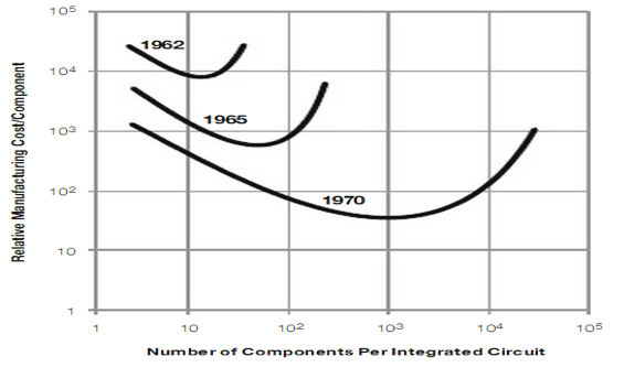
“The complexity for minimum component costs has in-creased at a rate of roughly a factor of two per year. Certainly over the short term this rate can be expected to continue, if not to increase. Over the longer term, the rate of increase is a bit more uncertain, although there is no reason to believe it will not remain nearly constant for at least 10 years”
The public information we now have indicates that:
a. The 28nm node is quite mature and we cannot expect that optimum integration vs. yield will double for it.
b. All that we know about the more advanced nodes (22/20nm, 16/14nm, …) indicates that the cost per transistor is not going to be reduced significantly vs. that of 28nm.
c. What we now know about embedded SRAM (“eSRAM”), I/O and other analog functions, indicates that most SoCs will end up at a higher cost as compared to 28nm.
Let’s recap using a few public charts to help tell the story of how we have reached that conclusion.
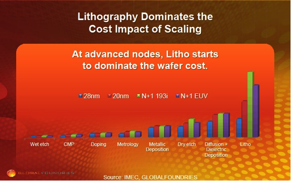
It starts with the escalating cost of lithography as illustrated in this 2013 chart from GlobalFoundries:
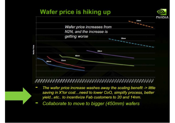
We should mention here that based on information released during last week’s SPIE Advanced Lithography (2014), it seems EUV is not going to be ready for the N+1 node (10nm). These costs, as well as other capital costs, increase, and thus drive up the wafer price as illustrated by the recent NVidia chart from Semicon Japan (Dec. 2013) below:
This escalating wafer cost eats away the higher transistor density gains, as articulated by NVidia and calculated by IBS’ Dr. Handel Jones and shown in the following table:

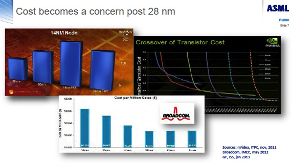
This is nicely illustrated by ASML slide from Semicon West (2013) below:
But this is just the smaller part of the problem. Advanced Integrated Circuits comprise far more than just logic gates. An SoC today contains a significant amount of embedded memories, I/Os and other support analog functions. Further, they include a large number of drivers and repeaters to reduce the RC delays that are escalating due to dimensional scaling. All of these scale very poorly.
The following chart was presented in an invited paper by Dinesh Maheshwari, CTO of Memory Products Division at Cypress Semiconductors, at ISSCC2014. It was also at the center of our recent blog “Embedded SRAM Scaling is Broken and with it Moore’s Law.”
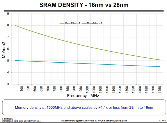
This chart shows that eSRAM scaling is ~1.1X for decent performance as compared to ~4X for logic gates. The chart below (from Semico Research) shows that an average SoC has more than 65% of its die area allocated to eSRAM.
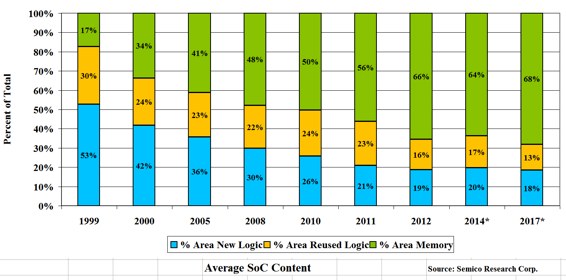
Consequently, the average SoC scaling to 16/14 nm could result in a significant cost increase, and hence 28nm is effectively the last node of Moore’s Law. To make things even worse, the remaining 35% of die area is not composed of only logic gates. More than 10% of the die area is allocated to I/O, pads and analog functions that either scale poorly or do not scale at all. And even in the pure logic domain scaling could not reach the potential 4X density improvements. The following chart was presented by Geoffrey Yeap, VP of Technology at Qualcomm, in his invited paper at IEDM 2013:
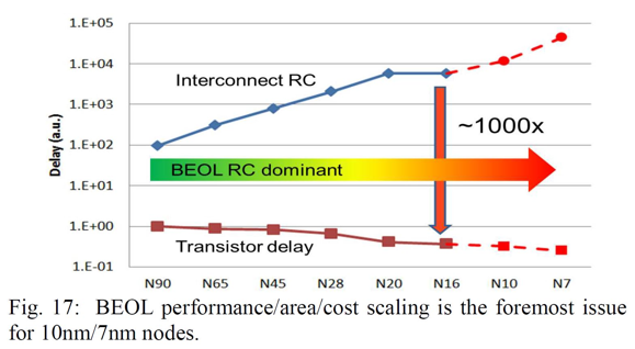
It illustrates the escalating interconnect RC delay with scaling – about 10X for two process nodes. This escalating RC delay eats away a significant part of the increase in gate density due to the exponential increase in buffer and driver counts and a similar increase in ‘white’ area kept for post layout buffer insertion, etc.
Final note: it seems clear that dimensional scaling has now reached negative returns, as is illustrated by the following GlobalFoundries chart:
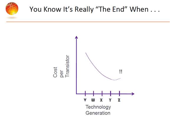
The time is now to look for other alternatives, among which monolithic 3D seems a most compelling option. It allows us to leverage all our current silicon knowledge and infrastructure while continuing with Moore’s Law by scaling up at 28nm.