In the process of competing with TSMC, which is at the forefront of technology, Samsung has finally taped a 3nm chip using its GAA transistor architecture.
This requires a design and certification tool different from the FinFET transistor structure used by TSMC and Intel, so Samsung uses Synopsys' fusion design platform. The physical design kit (PDK) for the process was released in May 2019 and was certified for the process last year.
It is a collaboration between Synopsys and Samsung, which aims to provide a highly optimized reference method for GAA process.
The reference design process includes an integrated RTL to GDSII design process supporting golden signoff and golden signoff products. The process is aimed at customers who want to use 3nm GAA process for chips in high performance computing (HPC), 5g, mobile and advanced artificial intelligence (AI) applications.
Sangyun Kim, vice president of Samsung OEM design technology team, said: "Samsung OEM is the core of promoting the next stage of industry innovation. We continue to develop process technology to meet the growing demand of professional and wide market applications. At Samsung Electronics. Our latest and advanced 3nm GAA process benefits from our extensive cooperation with Synopsys. The fusion design platform accelerates the preparation to effectively realize the commitment of 3nm process, proving the importance and benefits of these key alliances. "
Samsung said that the GAA architecture improved electrostatic characteristics, thereby improving performance and reducing power consumption, and brought additional benefits of new optimization opportunities for extra vectors based on NanoChip width control. Used with sophisticated voltage threshold tuning, this provides more ways to optimize the power, performance or area (PPA) design.
The design process also includes support for complex layout methods and layout planning rules, new routing rules, and increased variability. The process is based on a single data model and uses a common optimization architecture rather than a combination point tool.
Shankar Krishnamoorthy, general manager of digital design at Synopsys, said: "the GAA transistor structure marks a key turning point in technological progress, which is crucial to maintaining the scaling trajectory needed for the next wave of ultra large scale innovation."“ Our strategic partnership with Samsung foundry supports the delivery of state-of-the-art technologies and solutions together to ensure the continuation of these expansion trends and related opportunities for the broader semiconductor industry. "
Synopsys technical documents can be obtained from Samsung factory for 3 nm GAA technology process.
Fusion design platform includes fusion compiler for digital design, IC compiler II layout and routing, design compiler RTL synthesis, primetime timing signature, starc extraction signature, IC validator physical signature and silicon Smart Library representation.
Extended reading: Samsung will introduce GA at 3nm, TSMC at 2nm?
According to reports, there are two variants of the 3nm process - 3gaae and 3gaap - representing the early and plus, which are two designs based on nanosheet structures with multiple transverse striplines in the fins. This kind of NanoChip design has been discussed by IMEC as a follow-up product of FinFET, and has been studied by IBM in cooperation with Samsung and global foundries.
"Applying the GAA architecture to our next-generation process nodes will enable us to take the lead in opening up a new intelligent connected world, while strengthening our technology leadership," said Charlie BAE, executive vice president and head of OEM sales and marketing at Samsung.
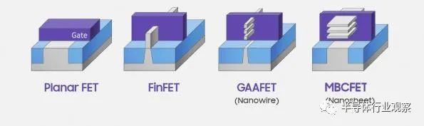
Gate all around (GAA) is sometimes called transverse nanowire FET. This is a FinFET surrounded by a gate. According to the expert's opinion, GAA transistor can provide better static characteristics than FinFET, which can meet the needs of some gate width. This is mainly reflected in the same size structure, the channel control ability of GAA is enhanced, so it is possible to further reduce the size; In traditional FinFET, only three sides of the channel are surrounded by the gate. In GAA, for example, the whole outer profile of the channel is completely wrapped by the gate, which means that the gate has better control performance over the channel.
Samsung researchers will call their 3 nm CMOS technology, which uses full ring gate (GAA) transistors, multi bridge channel (MBC) architecture. According to reports, the channel made of the horizontal layer of nanosheets is completely surrounded by the gate structure.
Samsung claims that the technology is highly manufacturable. Because it uses about 90% of the company's existing FinFET manufacturing technology, and only needs a small amount of modified photomask. They used it to build a fully functional high-density SRAM macro. They say the process has excellent gate controllability (65 MV / DEC subthreshold swing), which is 31% higher than the company's FinFET technology, and because the channel width of the nanosheet can be changed by direct patterning, this provides flexibility for the design.
For TSMC, gate all around FETs (gaafets) is still a part of its development roadmap. The company is expected to use new transistors in its "post N3" technology (possibly N2). In fact, the company is in the exploratory mode of the next generation of materials and transistor structures that will be used for many years to come.
"For advanced CMOS logic, TSMC's 3nm and 2nm CMOS nodes are well under way," the company said in its recent annual report“ In addition, TSMC has strengthened its exploratory R & D work, focusing on nodes beyond 2nm, 3D transistors, new memories and low-r interconnect, which are expected to lay a solid foundation for many technology platforms.
It is worth noting that TSMC is expanding the R & D and operation capacity of Fab 12, and is currently researching and developing N3, N2 and more advanced nodes.
Previous:
Next :